
🏆 PCB Design Gotcha Awards!
In this series, I will be listing a multitude of things that can "bite you" in your design workflow. These oversights can often get overlooked (even by seasoned professionals), especially on very complex designs.
Phillip Restall
9/2/20252 min read


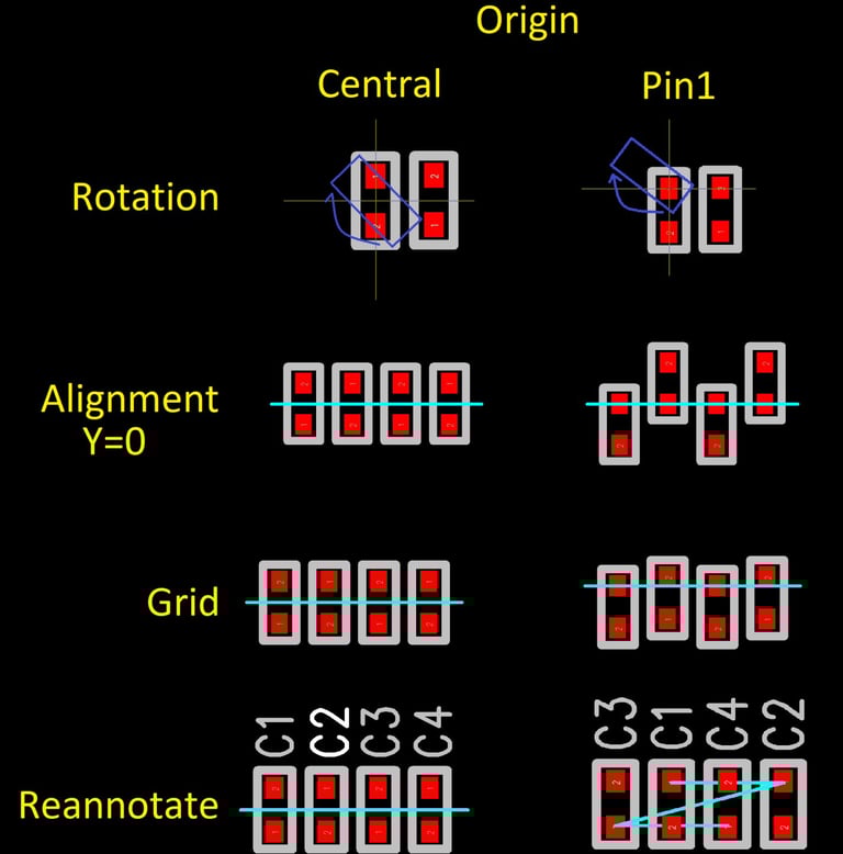
🏆 Centrally locating your PCB component Origin 👍 .
When creating your first PCB library, the decisions you make here can haunt you for years to come.
Something as simple as placing your origin can cost you many man hours throughout your design process.
Here are some of the reasons why having a centrally located origin is king 👑 vs using pin1:
✅ Rotating Components.
Components rotated around pin1 will no longer be in the correct location and you will need to do an additional move process.
✅ Alignment.
Many tools will allow you to align components by axis based on the component origin. This may not work out well if the origin is pin1.
✅ Grids.
Depending on your component, after rotating by pin1 origin, you may have to change your grid to make the component line up with others.
✅ Reannotation.
After your board is complete, you may want to reannotate your board. Setting pin1 as your origin can cause your components to be out of sequence.
✅ Compatibility.
Good third party libraries will conform to IPC7351, so if you pull in other components, it's useful if you are using the same formats.
🏆 Centrally locating your PCB Component Origin 👍 .
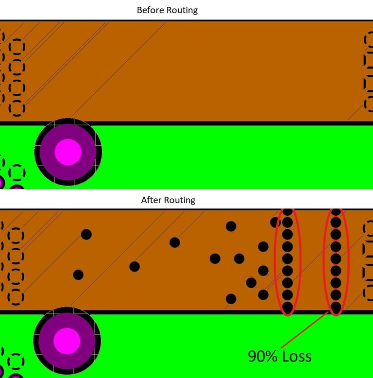
🏆 Always check stitching vias through critical power planes after routing!
Scenario-
You've started doing everything right:
✅ Worked out how much current is required for a set of pins.
✅ Calculated how thick your plane area needs to be.
✅ Connected your power source and target pins with a more than adequate plane area.
❌ Rechecked the area after routing.
As you can see from the example below, the area in question after routing has a massive 90% loss in current due to vias being routed in the plane area, which would have been catastrophic to the design.
🏆 Always check stitching vias through critical power planes after routing!
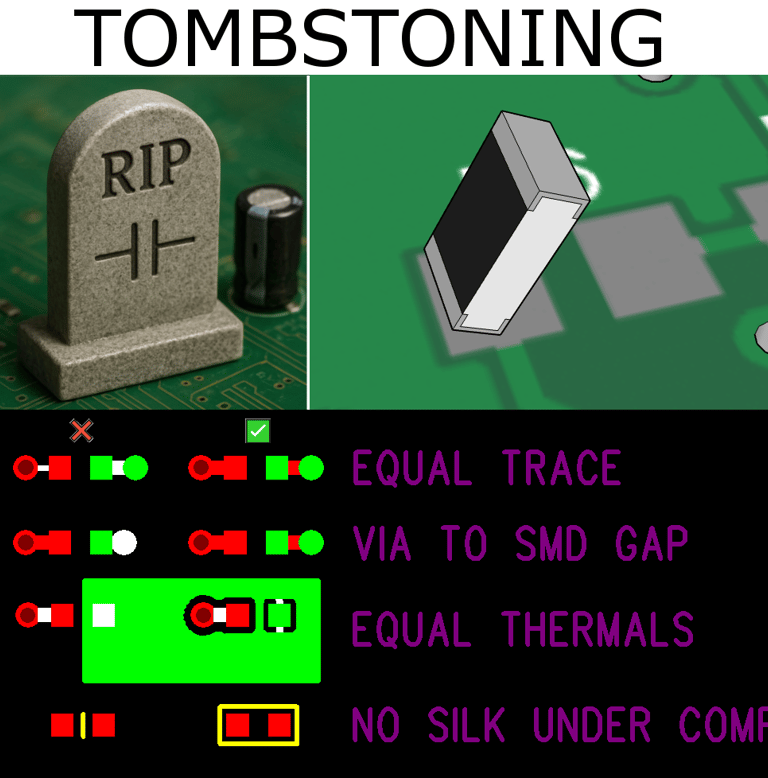
🏆 Reduce the likelihood of tombstoning 👍 .
Tombstoning is a surface-mount soldering defect on a PCB, where a component like a resistor or cap stands upright instead of lying flat during assembly. This occurs when the solder on one end of the component melts and wets before the other, causing surface tension to pull the component upright.
While designing your PCB and where your design allows, there are some things you can avoid doing to reduce the chances of this happening.
✅ Equalise your trace thickness on each pad of the device so they are balanced.
✅ Equalise your via to pad distances so they are the same.
✅ While connecting your pad to a plane, try to make the thermal reliefs total the other pad's trace thickness.
❌ Do not place silkscreen under the component footprint. Silkcreen can have a thickness and lift the device slightly in some cases.
🏆 Reduce the likelihood of tombstoning 👍 .
CAPABILITIES AND SERVICES
Contact
info@cadextreme.com
© 2026. All rights reserved.
PCB Layout Designs 50 LAyers+
Rigid, Flex, Flex-rigid, HDI, High-speed, Power boards
Blind/buried vias
Library Creation
Project migration
Schematic updates
3d modeling and technical drawing
Altium (PCB / Schematic)
Siemens Xpedition (PCB / Schematic)
Siemens PADs (PCB / Schematic)
Cadence Allegro / Orcad (PCB / Schematic)
SolidEdge (3d)
Solidworks (3d)
Autocad (2d)
main software supported